Pack power
B. Jayant Baliga came to NC State University in 1988, fresh off the success of a truly world-changing invention during his time as a researcher at General Electric.
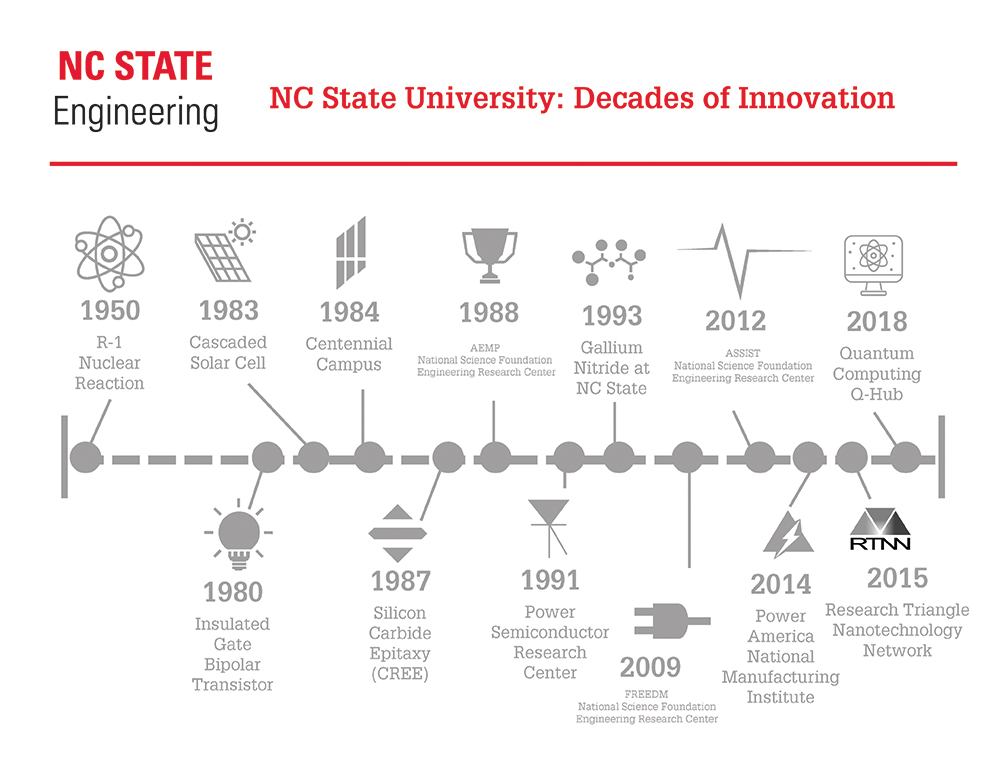
In 1980, Baliga invented the insulated gate bipolar transistor, a more-efficient high-power semiconductor switch that has saved humankind trillions of dollars in energy costs with its implementation in lighting, automobiles and manufacturing. Today Baliga, Progress Energy Distinguished University Professor in NC State’s Department of Electrical and Computer Engineering (ECE), still calls 1980 his “big year.”
It was also the year in which he began pursuit of another research question, one that he’s been working on ever since — what would the next power semiconductor material be?
“No one had bothered asking that question because everyone seemed quite happy with using silicon,” he remembered.
Silicon, because of its versatility and wide availability, has been the element of choice for semiconductors since the rise of the transistor in the middle of the 20th century. In the 1980s, some researchers had begun looking at the viability of other semiconductor materials, like silicon carbide (SiC) and gallium nitride (GaN).

After 15 years at General Electric, Baliga was considering a career switch to academic research and teaching. He was drawn to NC State, in part, by work already happening in Robert Davis’ lab in the Department of Materials Science and Engineering (MSE) to grow SiC crystals and wafers, a tricky proposition because the material is difficult to work with. Baliga thought he could leverage that work if he accepted a position at NC State.
Over the decades since, work in the College of Engineering on SiC and GaN, known as wide bandgap (WBG) semiconductors, has led to spinoff companies including Cree and later Wolfspeed, Adroit Materials, HexaTech and Kyma Technologies, and has put NC State in position to lead national research centers working in these areas.
Wide bandgap semiconductor devices are able to operate at higher voltages, frequencies and temperatures and are more efficient than current silicon semiconductors. As they become more cost competitive, wide bandgap semiconductor devices are being increasingly used in military applications, renewable energy infrastructure, communications, radar and more because of size, weight and power-efficiency advantages.
Commercial Leap Ahead for Wide Bandgap Semiconductors (CLAWS) is the latest research effort in this area led by NC State. CLAWS is a Department of Defense (DoD) Microelectronics Commons hub executed through Naval Surface Warfare Center Crane Division and the National Security Technology Accelerator (NSTXL) to bring lab to fab prototyping and critical microelectronics technology areas such as WBG semiconductor devices to the market for both military and commercial uses. In 2023, NC State was awarded an initial $39.4 million for the first year of a five-year program to lead the center, which also includes North Carolina Agricultural & Technical State University and six industry partners.
The funding is part of a $238 million initial investment through the Creating Helpful Incentives to Produce Semiconductors (CHIPS) and Science Act for the establishment of eight Microelectronics Commons hubs spread across the United States. In addition to the hub funding, the CLAWS program is competing for additional funding for advanced semiconductor projects for the DoD.
“The technologies hold the potential to enable future electric vehicles, power grid technologies, 5G/6G, quantum technologies and artificial intelligence applications,” said Fred Kish, M.C. Dean Distinguished Professor in ECE and the director of the new hub. “They are also important for national security applications by providing energy efficiency, size, weight, power and performance advantages in critical application areas including weapons systems, warfighter outfitting, position/navigation/timing, biotechnical and medical, materials processing, displays and a host of additional defense needs.”
A history of leadership
Baliga established the Power Semiconductor Research Center at NC State in 1991 to work on research with companies around the globe on power semiconductor device technology for use in motor drives, cellular communication, hybrid and electric vehicles, robotics and more.
Semiconductor work at NC State received a major boost in 2008, when the University was awarded the lead in a National Science Foundation (NSF) Engineering Research Center dedicated to building a new smarter electric grid that can incorporate renewable energy sources. The NSF Future Renewable Electric Energy Distribution and Management (FREEDM) Systems Center has developed a working smart-grid system and the technologies that underpin it: a solid-state transformer that allows bi-directional power flow and removes the need to convert direct current to alternating current for home use; a more efficient fault-isolation device; and the controllers and algorithms that allow them to work together. FREEDM’s research thrust areas include one focused on the development of WBG devices for utility scale applications in the new smarter grid.
This track record of research center leadership put NC State in a strong position to lead another new federally funded center, this one a member-driven manufacturing consortium dedicated to commercialization of WBG power devices and tasked with developing a commercial foundry for the development of SiC and GaN chips. PowerAmerica was one of several sites in the Manufacturing USA network established by President Barack Obama’s administration, and the former president visited the NC State campus in 2014 to announce its creation.
The Department of Energy renewed funding for PowerAmerica for another five years in 2023. Since its inception, the center has commercialized more than 10 WBG technologies. Through its education and workforce development program, it has trained hundreds of master’s and Ph.D. students — and thousands more K-12 students in STEM programs.
Eliminating barriers
The CHIPS and Science Act recognizes the need for the United States to be a global leader in production of the semiconductor chips that will power the most important industries of the future, including renewable energy, quantum computing and artificial intelligence. As one of eight microelectronics hubs, CLAWS will eliminate existing barriers that inhibit domestic U.S. semiconductor innovations from moving efficiently to production, said John Muth, Distinguished Professor in ECE and principal investigator for CLAWS.
Those barriers include limited access to advanced wafers and epitaxy, fabrication processes and packaging technologies, in addition to high costs for both intellectual property and electronic design automation licenses as well as for process and metrology tooling to support manufacturing. Lack of available workforce talent and expertise is also a barrier, as is lack of access to existing fabrication facilities for prototyping.
CLAWS operates under a “lab to fab” model, establishing a research foundry on NC State’s campus that will work with industry to make research development kits to accelerate device development and transfer the process to industrial core foundries that have the ability to manufacture the devices in the volumes needed for DoD or civilian applications. This hub and core model helps cross a so-called “valley of death” that prevents many lab technologies from reaching production. CLAWS will also include a strong education and workforce development program that will include undergraduate research, summer programs for high school and community college educators and specialized short courses for the industry workforce.
CLAWS research will include ultrawide bandgap (UWBG) semiconductors such as diamond and gallium oxide, which can operate at even higher voltages. Previous research work in NC State MSE on UWBG devices has led to start-up companies.
General Electric is one of six CLAWS industry partners. Decades of NC State research expertise and the University’s track record of leadership make working with the new center an easy choice.

“GE Aerospace is excited to partner with NC State on the CLAWS hub to develop the next generation of WBG and UWBG devices for DoD and their customers,” said Reza Ghandi, principal engineer at GE Global Research. “Together, we are creating a national R&D and prototyping powerhouse in the United States for wide bandgap and ultrawide bandgap devices to accelerate lab-to-fab transitions for these critical technologies. Both GE and NC State have a long history in this field with complementary areas of expertise that will strengthen America’s overall competitiveness in semiconductor technology.”
Like all of the new Microelectronics Commons hubs, CLAWS will address the barriers that keep university researchers and startups from taking technology all the way to commercial adoption.
“With CLAWS, we are creating this bridge between research and development and commercialization,” Baliga said. “There’s a need for a place like that.”